"I should point out up front that I have no formal training
in NMOS or any other chip design technology, hence the disclaimer
attached to my notes! I believe the transistor-like symbols
represent nMOS pass-gates, ie FETs used as a switchable bi-directional
channel."
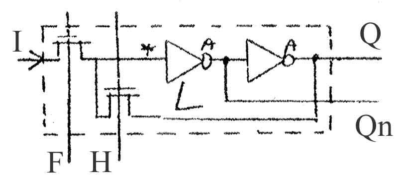
"The "L" block implements an inverter-based
latch, using nMOS pass-gates driven by complimentary signals to
switch between "follow" and "hold" mode. Research
indicates that this is a very common latch used in VLSI CMOS design."
So, in the diagram above I would be the input, F the follow
control, H the hold control, and Q/Qn the outputs. When F is high
the output Q follows in input I. Qn will always be the complement
of Q. When F goes low and H goes high the output Q will get looped
back to the input of the first inverter thus holding the state of
the input.
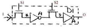
"The delay blocks (D1 - single input, D2 - dual input, D1R -
single input with reset) and the delay latch DL are all driven by
a bi-phase clock and operate as "dynamic" logic blocks.
Taking D1 as an example, when @1 (phase-1 clock
line) [S1 in the diagram] is high the input
pass-gate allows the input signal (ground or Vdd) to directly drive
the first inverter. Assuming the inverter consists of a FET and a
pull up resistor (usually implemented as a second FET hard-wired on),
this will charge or discharge the "parasitic storage capacitor"
formed by the FET gate inside the inverter.
As @1 [S1 in the diagram] goes
low the input pass-gate goes into high impedance state leaving the
inverter's gate capacitor in either a fully charged (representing
"0") or fully discharged (representing "1") state.
Since @2 (phase-2 clock line) [S2 in the diagram]
is low the output pass-gate is also high impedance at this time. Although
the gate capacitor is subject to leakage, for a short period it will
hold its charge.
As long as @2 [S2 in the diagram]
goes high before the gate charge drains away and the first inverter
floats high, the second inverter will take on its current value and
propagate it to the output of the logic block for a short time - long
enough for the next clocked logic block to latch or make use of the
data.
I'm not sure exactly what the * denotes but it only appears
where these pass-gates are used (although not all gates have them).
My original thought was it indicates where a data value is considered
to be "stored" for a full bi-phase cycle, but it may indicate
where pass-gates are built into the adjacent logic gate (I have
seen this practice mentioned) or something else entirely!"
So to summarize the D1 (Delay 1 input) block, when S1 goes high
the input I will be passed through the first inverter to the second
FET. When S1 goes low and S2 goes high the input value will be passed
through the second inverter to the output.
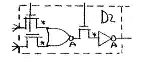
The D2 (Delay 2 input) block is the same as the D1 block except
that is has two inputs. A high on either input will be passed though
to the output.
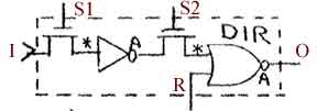
The DIR (Delay 1 with Reset) block is similar to the D1 block but
has a reset input. As long as R is held high the output will always
be kept low. When R is held low, this will behave just like the
D1 block.
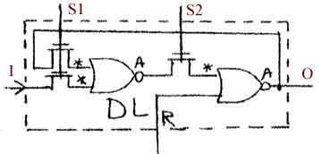
The DL (Delay Latched) block is similar to the DIR block but with
latching capability. When the input (I) is set high and S1 and S2
are clocked in sequence the high will appear on the output (O) and
will also be fed back to the input so even if I goes low and S1
and S2 are clocked, the output will remain high. To clear the output
R must be set high and S1 must be clocked high.
